ups
DIY UPS VRLA Battery Controller for ESP32C3, ESP32, M5Stack Core
Network devices and servers connected to USB ports will continue to operate even in power outage.
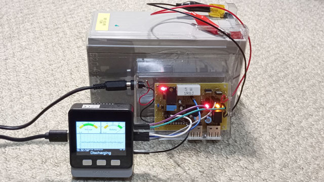
Fig. DIY UPS System Using M5Stack Core and 12V 7.2Ah VRLA Battery
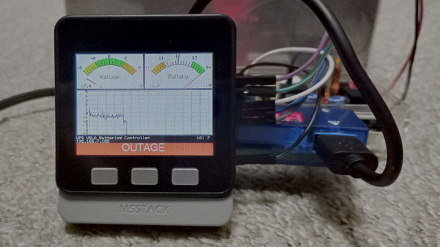
Fig. Server Continuity Plan in Power Outage
WARNING
I do not take any responsibility for safety. For example, mishandling batteries may result in danger to your life or loss of your property.
Instruction
The instruction page for this system is on my blog written in 日本語 and some languages translated by Google Translate:
https://bokunimo.net/blog/esp/4320/
Supported MCUs
- for ESP32C3 in the folder “esp32c3”
- for M5Stack Core in “m5core”
- for ESP32 is in “atom”
Features
- for 12V VRLA Batteries
- Level Meters show Charging/Discharging Power and Battery Voltage
- USB Type A Female Output Ports, 5V 500mA
- the Ambient; the web monitor service shows visible charts such as the sensor values
- LINE Notify; a message notification service on the LINE platform
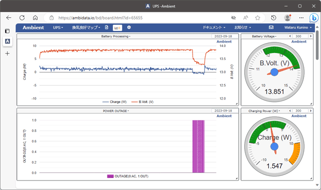
Fig. Web Service the Ambient for Monitoring Sensor Values
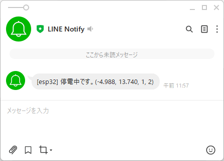
Fig. LINE App Gets Message from the UPS
DIY UPS Schematic for M5Stack Core
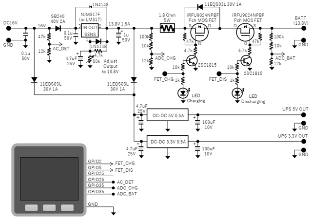
Fig. Schematic of DIY UPS Battery Controller for M5Stack Core
Hardware Adjusting CV Charging Voltage
This charging system use CV; constant voltage charging, with current limit resistor 1.8 Ohm.
The CV Charging Voltage is set using a 50k Ohm variable resistor by manually.
Please adjust the output voltage is NOT over 13.8 V or under 10.8V.
For the example setting from 12.0 V to 13.8 V, if it is set 12.0 V, the backup time in outage might be shorter.
But if sets 13.8V, the battery life might be shorter than 12.0 V setting.
This CV charging method takes many days to charge after a power outage.
If you want to charge it more quickly, please temporarily increase the charging voltage.
Software Definition ADC_CHG_DIV and ADC_BAT_DIV
The values of definition ADC_CHG_DIV and ADC_BAT_DIV on the source files need to be adjusted.
These are the voltage divided factors for the voltage measurements.
ADC_CHG_DIV is for the output voltage of NJM317F regulator for battery charging, and ADC_BAT_DIV is for the battery voltage.
If you put the resistors 100k, 10k, and 12k which have enough tolerance to measure, these values are calculated as below.
#define ADC_CHG_DIV 12./(110.+12.)
#define ADC_BAT_DIV 12./(110.+12.)
But generally, resistors have an error tolerance of +/-5% or +/-1%. So, you need to adjust the definition values.
- Measure the output voltage of NJM317F, the value is for the denominator of ADC_CHG_DIV.
- Measure the divided voltage of NJM317F by resistors at ADC_CHG. The value is for the numerator of ADC_CHG_DIV.
- In a similar way, measure for ADC_BAT_DIV at BATT and ADC_BAT.
-
Edit the values like a below example.
#define ADC_CHG_DIV 1.353 / 13.78
#define ADC_BAT_DIV 1.363 / 13.72
How to Start
- Adjust Charging Voltage
- Set Definition
- Write the software to your target MCU.
- Check the voltage of a VRLA battery. If it is under 10.8V, please use another new battery.
- Connect the battery to the controller board.
- Plug the AC Adaptor.
Note: If you plugged the AC supply before connecting the battery, this system isn’t going to be started, please disconnect the AC, and connect the battery before the AC.
Overview of Assigned GPIO Pins
2 of ADC Input Pins used for Voltage and Current Measurement
One of the ADC is for battery voltage measurement.
The other is for measuring the charging or discharging current of the battery via a small resistor.
Circuits for ADC Inputs
Series R=110k Ohm and R=12k Ohm resistors divides the battery voltage to 1/10.
On the above circuit schematic, 110k Ohm are structed by 100k Ohm one and 10k Ohm.
Input on a GPIO used for Detecting Outage
This GPIO input is used to detecting power outage in your home. Series R=47k Ohm and R=12k Ohm resistors divides the 16V output of AC adapter to 3.3V.
Outputs of 2 GPIOs used for Switching Charging or Discharging
Two of the series FETs switches the connection modes of the charging, the discharging, and disconnected mode.
In the charging mode and the discharging mode, the both of FETs are turned On.
And if the voltage of battery reached too high voltage for CV charging, turned Off the charging FET.
Both FETs are turned off to prevent over-discharge when the voltage drops below the end voltage.
Pinout for M5Stack Core
| GPIO | Direction | to |
|---|---|---|
| 2 | Output | Charging FET |
| 5 | Output | Discharging FET |
| 26 | Input | Outage Detector |
| 35(ADC1_7) | Input | Charger Voltage |
| 36(ADC1_0) | Input | Battery Voltage |
Pinout for ESP32C3
| Pin | 割当 | 接続 | Pin | 割当 | 接続 | |
|---|---|---|---|---|---|---|
| 1 | 3V3 | Power(3.3V) | 18 | IO 0 | NA(or GND) | |
| 2 | EN | 17 | IO 1 | Outage Detector(USER SW) | ||
| 3 | IO 4 | Charging FET | 16 | IO 2 | Charger Voltage(ADC1_2) | |
| 4 | IO 5 | Discharging FET | 15 | IO 3 | Battery Voltage(ADC1_3) | |
| 5 | IO 6 | 14 | IO19 | (I2C SCL) | ||
| 6 | IO 7 | 13 | IO18 | NA(or GND) | ||
| 7 | IO 8 | Pull Up, RGB LED | 12 | TXD | ||
| 8 | IO 9 | 11 | RXD | |||
| 9 | GND | Power(GND) | 10 | IO10 | (I2C SDA) |
Functional Design for 12V VRLA Batteries
12V VRLA Batteries are structed series 6 cells, and each cells work if the cell voltages meet to 2.0V or between 1.8V to 2.3V. This is CV charging system for UPS, so the charging voltage is set to 13.8V. And the stopping voltage for charging is set to 14.7, it’s protected from unexpected higher voltage, such as breakdown circuits.
| Mode | Battery Voltage | Function | Condition |
|---|---|---|---|
| Charging | 2.3 x 6 = 13.8V | Stop Charging | Over 14.7V |
| Fatal | 1.8 x 6 = 10.8V | Disconnect | Under 10.8V |
by 国野 亘 Wataru KUNINO
- ウェブサイト https://bokunimo.net/
- ブログ https://bokunimo.net/blog/
- ESP32メニュー https://bokunimo.net/blog/menu/esp/
- M5Stackメニュー https://bokunimo.net/blog/menu/m5stack/
GitHub Pages by bokunimo.net
-
(This Document)
https://git.bokunimo.com/ups/ -
M5Stack
https://git.bokunimo.com/m5/